These are the ramblings of Matthijs Kooijman, concerning the software he hacks on, hobbies he has and occasionally his personal life.
Most content on this site is licensed under the WTFPL, version 2 (details).
Questions? Praise? Blame? Feel free to contact me.
My old blog (pre-2006) is also still available.
See also my Mastodon page.
- Raspberry pi powerdown and powerup button (45)
- Repurposing the "Ecobutton" to skip spotify songs using Linux udev/hwdb key remapping (3)
- How to resize a cached LVM volume (with less work) (2)
- Reliable long-distance Arduino communication: RS485 & MODBUS? (6)
- USB, Thunderbolt, Displayport & docks (21)
| Sun | Mon | Tue | Wed | Thu | Fri | Sat |
|---|---|---|---|---|---|---|
| 1 | 2 | 3 | 4 | 5 | 6 | 7 |
| 8 | 9 | 10 | 11 | 12 | 13 | 14 |
| 15 | 16 | 17 | 18 | 19 | 20 | 21 |
| 22 | 23 | 24 | 25 | 26 | 27 | 28 |
(...), Arduino, AVR, BaRef, Blosxom, Book, Busy, C++, Charity, Debian, Electronics, Examination, Firefox, Flash, Framework, FreeBSD, Gnome, Hardware, Inter-Actief, IRC, JTAG, LARP, Layout, Linux, Madness, Mail, Math, MS-1013, Mutt, Nerd, Notebook, Optimization, Personal, Plugins, Protocol, QEMU, Random, Rant, Repair, S270, Sailing, Samba, Sanquin, Script, Sleep, Software, SSH, Study, Supermicro, Symbols, Tika, Travel, Trivia, USB, Windows, Work, X201, Xanthe, XBee
 &
&
(With plugins: config, extensionless, hide, tagging, Markdown, macros, breadcrumbs, calendar, directorybrowse, feedback, flavourdir, include, interpolate_fancy, listplugins, menu, pagetype, preview, seemore, storynum, storytitle, writeback_recent, moreentries)
Valid XHTML 1.0 Strict & CSS
Last year, I got myself an Atmel JTAGICE3 programmer, in order to speed up programming my Pinoccio boards. This worked great, except that as can be expected of the tiny flatcable they used (1.27mm connector and even smaller flatcable), the cable broke within 6 months.
Atmel support didn't want to replace it, because it wasn't broken when I first unpacked the programmer, and told me to find and buy a new cable myself. Since finding these cables turns out to be tricky, and I didn't feel like breaking another cable in 6 months, I designed a converter board.
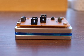
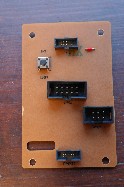
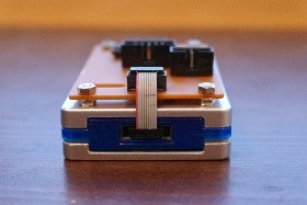
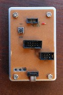
This board is a PCB to be mounted on top of the JTAGICE3, which can be connected permanently to the JTAGICE3 using a very short (1") flatcable, and converts to a "normal" (2.54mm pitch) connector for every-day use. It has both 10-pin JTAG and 6-pin ICSP headers, replacing the two converters that atmel ships. Additionally, the board has another 1.27mm pitch connector, so you can still connect target boards which also use this tiny connector. This still requires using a fragile cable, but now at least only when it's really needed. Finally, the board has a reset button, which can be used to reset the target board (useful for Pinoccio boards, which have none themselves).
Connector polarity
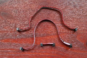
One odd thing about the JTAGICE3 is that the connector on the programmer itself is reversed wrt the polarity notch. Most flatcable connectors have a polarity key, with a matching notch in the socket, to prevent reversing the connector. Normally, the key and notch are at the side that has pin 1, but the JTAGICE3 has it reversed (rotated), so it's on the side that has pin 2. The flatcable that Atmel supplies also has one of the connectors reversed (it's actually upside down), which cancels out this reversion again.
This reversion actually makes it even harder to get a replacement cable, since most of the cables you can find in this size have both connectors applied normally.
Since I didn't want any of this reversed socket business on my board, I made sure to do the reversion in the cable between the JTAGICE3 and the converter board, and have all sockets on the board using the normal orientation.
This does mean that the original cable supplied by Atmel is now useless, even it hadn't broken, since it's way too long to connect the JTAGICE3 to the converter board, but connecting the converter board to a target that uses this tiny connector, needs a "straight" cable. The same goes for the squid cable, though that can still be used by manually correcting the pin numbers (1 becomes 10, 2 becomes 9, etc.).
Note that if you do want to keep using the reversed cable supplied by Atmel (perhaps because yours hasn't broken yet), that's just a matter of soldering on the JTAG2 socket rotated 180° (the notch is towards the board edge instead of toward the middle) - no need to change the PCB.
Above, there's a photo of the various flatcables. From top to bottom: original cable, with one connector upside-down, new regular cable, short cable with one connector reversed (effectively the same as upside-down).
Parts
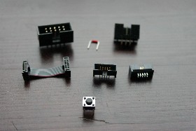
So, for this project, I needed:
- a custom-designed PCB
- a 2x5 pin shrouded pin header, regular 2.54mm spacing
- a 2x3 pin shrouded pin header, regular 2.54mm spacing
- two 2x5 pin shrouded pin headers, 1.27mm spacing (Samtec SHF-105-01-L-D-TH)
- a tiny, reversed flatcable (Samtec FFSD-05-D-01.00-01-N-RN2)
- a longer, non-reversed flatcable (Samtec FFSD-05-D-06.00-01-N)
- Some jumper wire
- Some bolts, nuts, copper standoff and insulating rings
For the half-pitched flatcables and connectors, I found that Samtec manufactures parts that fit the bill (though there should be others as well). I used their SHF series for the sockets, and FFSD series for the cables. Since I had some peculiar requirements (1" cable, reversed polarity key) and digikey only stocks a very limited number of products from their line, I ended up ordering what I needed as (free) samples from Samtec directly. There, you can just specify whatever parameters you need (once you figure out their part number system). Given the cables took a few days longer to ship, I believe they assembled them on demand for me. Thanks, Samtec!
Board design and milling
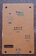
I designed the board in Kicad, my favorite open-source schematic and board tool. I had to design a custom footprint for the 1.27mm pitch connector, modify some other footprint to get 3mm mounting holes and I already had custom AVR-ICSP and AVR-JTAG pin header components (just normal headers, but with named pins), all else is just standard kicad stuff.
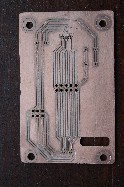
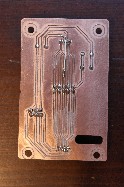
Since the board would cover up the status leds of the JTAGICE3, I added a cutout in the design, so you can still see the leds. I used pcb2gcode and a Mantis CNC mill to mill out the board, but I couldn't quite figure out how to get internal cutouts working properly. In the end, pcb2gcode would do the cutout, but it would mill on the outside of the cutout line instead of on the inside. I modified my design to shrink the cutout line by 1mm (size of my milling tool), so you might need to modify this line for your workflow if you want to create this board as well.
For connecting the 1.27mm connectors, I'm running traces in between the pins of the connector. This is really tiny stuff, which isn't conforming to my clearance requirements. This is intentional: If I reduced my clearance requirement or reduced the trace size, this would affect the traces everywhere on the board, not just the part where they run between the pins. By keeping the traces wide, pcb2gcode will also see a clearance violation but do its best to fulfill it by just milling exactly through the middle - which gives me the largest trace and pad size possible with my machine. You might need to modify this a bit for your workflow.
Because squeezing in these traces reduces the width of these pads significantly (in a few places they're no wider than the holes), I modified the footprint to make the pads a bit higher, so you at least have some area left for soldering.
After milling the board, and applying the silkscreen markings using a lasercutter, I realized I had forgotten markers for pin 1 on the connectors. I've fixed this in the design, for anyone else to benefit.
For a lot more info about milling PCBs using a Mantis CNC mill, see this page at fablabamersfoort. It's an ongoing report of my experiments. It is written in Dutch, though.
I made the board design available on github, for anyone else to play with.
Assembly
Soldering the board was easy, though some of the traces ended up a bit small because I'm running against the limits of my CNC mill. One trace actually got destroyed while soldering, so I fixed that using a piece of wire on the copper side.
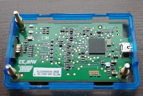
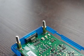
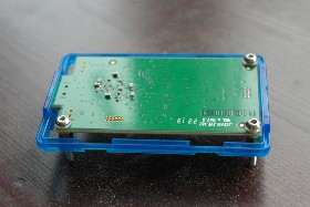
To mount the board on top of the JTAGICE3, I had to make a few modifications to the programmer. The original PCB in the JTAGICE3 already had three (unused) mounting holes, which I could conveniently use. I found some 8mm high copper standoffs, which together with a 1.5mm plastic ring (for insulation) fit snugly between the original PCB and the top of the casing.
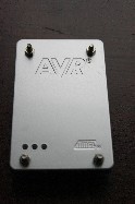
I slightly enlarged the mounting holes in the original PCB to 3mm, so I could fit standard M3 bolts. I also drilled 3mm holes in the top side of the casing, to match the mounting holes. I also needed to mill away a bit of plastic from the inside of the bottom casing, just below the three mounting holes, to make room for the head of the bolt.
To solidly fix the new board, I used a fourth mounting hole in my own PCB, which only attaches to the JTAGICE3 casing, not the original PCB.
During assembly, it turned out that my cutout was positioned slightly too high. I already corrected this in the board design I published, so that one should be good.
The end result is an elegant and solid extension of the programmer, with easily accessible connectors. There's still a tiny ribbon cable in there, but it fits perfectly and should never be under much stress. Now, back to actual work :-p



Comments are closed for this story.